- 您现在的位置:买卖IC网 > Sheet目录238 > NUP3115UPMUTAG (ON Semiconductor)TVS QUAD ARRAY LOW CAP 6-UDFN
�� �
�
�NUP3115UPMU�
�Transient� Voltage�
�Suppressors�
�Low� Capacitance� ESD� Protection� for�
�High� Speed� Data�
�The� three� ?� line� voltage� transient� suppressor� array� is� designed� to� protect�
�voltage� ?� sensitive� components� that� require� ultra� ?� low� capacitance� from�
�ESD� and� transient� voltage� events.� This� device� features� a� common� anode�
�design� which� protects� three� independent� high� speed� data� lines� and� a� V� CC�
�power� line� in� a� single� six� ?� lead� UDFN� low� profile� package.�
�Excellent� clamping� capability,� low� capacitance,� low� leakage,� and� fast�
�response� time� make� these� parts� ideal� for� ESD� protection� on� designs�
�where� board� space� is� at� a� premium.� Because� of� its� low� capacitance,� it� is�
�suited� for� use� in� high� frequency� designs� such� as� a� USB� 2.0� high� speed.�
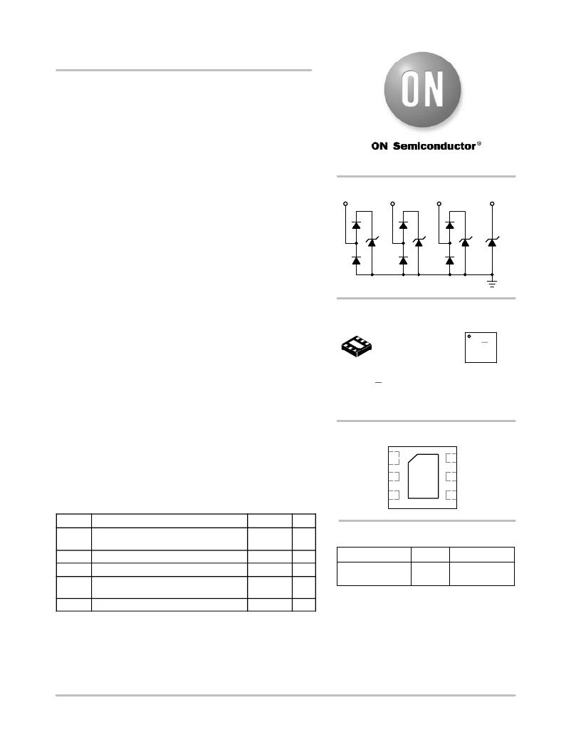
�D� 1�
�http://onsemi.com�
�D� 2� D� 3�
�6.8V� 6.8V�
�6.8V�
�V� CC�
�16V�
�1�
�6�
�D� 1� 1�
�D� 2� 2�
�Features�
�?� Low� Capacitance� 0.8� pF�
�?� UDFN� Package,� 1.6� x� 1.6� mm�
�?� Low� Profile� of� 0.50� mm� for� Ultra� Slim� Design�
�?� Stand� Off� Voltage:� 5.5� V�
�?� Low� Leakage�
�?� Protects� up� to� Three� Data� Lines� Plus� a� V� CC� Pin�
�?� V� CC� Pin� =� 15� V� Protection�
�?� D� 1� ,� D� 2� ,� and� D� 3� Pins� =� 6.4� V� Minimum� Protection�
�?� IEC61000� ?� 4� ?� 2:� Level� 4� ESD� Protection�
�?� This� is� a� Pb� ?� Free� Device�
�Typical� Applications�
�?� USB� 2.0� High� ?� Speed� Interface�
�?� Cell� Phones�
�?� MP3� Players�
�?� SIM� Card� Protection�
�1�
�MARKING�
�DIAGRAM�
�UDFN6� 1.6x1.6�
�MU� SUFFIX� P3� M� G�
�CASE� 517AP� G�
�P3� =� Specific� Device� Code�
�M� =� Date� Code�
�G� =� Pb� ?� Free� Package�
�(Note:� Microdot� may� be� in� either� location)�
�PIN� CONNECTIONS�
�6� V� CC�
�GND� 5� NC�
�MAXIMUM� RATINGS� (T� J� =� 25� °� C,� unless� otherwise� specified)�
�D� 3� 3�
�4�
�NC�
�Symbol�
�Rating�
�Value�
�Unit�
�I� PK�
�Peak� Pulse� Current� V� CC� Diode�
�8x20� m� sec� double� exponential� waveform�
�5.0�
�A�
�ORDERING� INFORMATION�
�T� J�
�Operating� Junction� Temperature� Range�
�?� 40� to� 125�
�°� C�
�Device�
�Package�
�Shipping� ?�
�T� STG� Storage� Temperature� Range� ?� 55� to� 150� °� C�
�T� L� Lead� Solder� Temperature� –� Maximum� 260� °� C�
�(10� seconds)�
�ESD� IEC� 61000� ?� 4� ?� 2� Contact� 8000� V�
�Stresses� exceeding� Maximum� Ratings� may� damage� the� device.� Maximum�
�Ratings� are� stress� ratings� only.� Functional� operation� above� the� Recommended�
�Operating� Conditions� is� not� implied.� Extended� exposure� to� stresses� above� the�
�Recommended� Operating� Conditions� may� affect� device� reliability.�
�See� Application� Note� AND8308/D� for� further� description� of�
�survivability� specs.�
�NUP3115UPMUTAG� UDFN6� 3000/Tape� &� Reel�
�(Pb� ?� Free)�
�?For� information� on� tape� and� reel� specifications,�
�including� part� orientation� and� tape� sizes,� please�
�refer� to� our� Tape� and� Reel� Packaging� Specification�
�Brochure,� BRD8011/D.�
�?� Semiconductor� Components� Industries,� LLC,� 2011�
�August,� 2011� ?� Rev.� 2�
�1�
�Publication� Order� Number:�
�NUP3115UPMU/D�
�发布紧急采购,3分钟左右您将得到回复。
相关PDF资料
NUP4000DR2G
TVS ARRAY BIDIR 400W 15V 8SOIC
NUP4004M5T1G
IC TVS ARRAY QUAD BIDIR 5TSOP
NUP4012PXV6T1G
TVS ARRAY QUAD LOW CAP SOT-563
NUP4060AXV6T1G
IC TVS ARRAY 4LINE SOT-563
NUP4102XV6T1G
IC TVS ARRAY QUAD BIDIR SOT-563
NUP4103FCT1
IC TVS ARRAY QUAD UNI 5FLIPCHIP
NUP4106DR2G
TVS LO CAP 500W 3.3V 8SOIC
NUP4114UCLW1T2G
TVS ARRAY QUAD UNIDIR SC88
相关代理商/技术参数
NUP4000
制造商:ONSEMI 制造商全称:ON Semiconductor 功能描述:Bi-directional TVS Array for High-Speed Data Line Protection
NUP4000DR2G
功能描述:TVS二极管阵列 4 CHAN BIDIRECTIONAL TVS RoHS:否 制造商:Littelfuse 极性: 通道:4 Channels 击穿电压: 钳位电压:11.5 V 工作电压:2.5 V 峰值浪涌电流:20 A 安装风格:SMD/SMT 端接类型:SMD/SMT 系列: 最小工作温度:- 40 C 最大工作温度:+ 85 C
NUP4004M5
制造商:ONSEMI 制造商全称:ON Semiconductor 功能描述:5−Pin Bi−Directional Quad TVS Array
NUP4004M5T1G
功能描述:TVS二极管阵列 5 PIN BIDRECTNL QUAD RoHS:否 制造商:Littelfuse 极性: 通道:4 Channels 击穿电压: 钳位电压:11.5 V 工作电压:2.5 V 峰值浪涌电流:20 A 安装风格:SMD/SMT 端接类型:SMD/SMT 系列: 最小工作温度:- 40 C 最大工作温度:+ 85 C
NUP4012PMUTAG
功能描述:TVS二极管阵列 LOW CAP TVS ARRAY RoHS:否 制造商:Littelfuse 极性: 通道:4 Channels 击穿电压: 钳位电压:11.5 V 工作电压:2.5 V 峰值浪涌电流:20 A 安装风格:SMD/SMT 端接类型:SMD/SMT 系列: 最小工作温度:- 40 C 最大工作温度:+ 85 C
NUP4012PXV6
制造商:ONSEMI 制造商全称:ON Semiconductor 功能描述:Quad Transient Voltage Suppressor Array
NUP4012PXV6T1G
功能描述:TVS二极管阵列 LOW CAP QUAD TVS ARRAY RoHS:否 制造商:Littelfuse 极性: 通道:4 Channels 击穿电压: 钳位电压:11.5 V 工作电压:2.5 V 峰值浪涌电流:20 A 安装风格:SMD/SMT 端接类型:SMD/SMT 系列: 最小工作温度:- 40 C 最大工作温度:+ 85 C
NUP4016
制造商:ONSEMI 制造商全称:ON Semiconductor 功能描述:Ultra-Low Capacitance Diode-TVS Array for High Speed Data Line Protection